Tag Archives: semiconductor

Microprocessors From Pencil Lead

UA physicists are making discoveries that may advance electronic circuit technology.

Graphite, more commonly known as pencil lead, could become the next big thing in the quest for smaller and less power-hungry electronics.

Resembling chicken wire on a nano scale, graphene – single sheets of graphite – is only one atom thick, making it the world’s thinnest material. Two million graphene sheets stacked up would not be as thick as a credit card. (more…)

Read More

Better Organic Electronics

*Berkeley Lab Researchers Show the Way Forward for Improving Organic and Molecular Electronic Devices*

Future prospects for superior new organic electronic devices are brighter now thanks to a new study by researchers with the U.S. Department of Energy (DOE)’s Lawrence Berkeley National Laboratory (Berkeley Lab). Working at the Lab’s Molecular Foundry, a DOE nanoscience center, the team has provided the first experimental determination of the pathways by which electrical charge is transported from molecule-to-molecule in an organic thin film. Their results also show how such organic films can be chemically modified to improve conductance.

“We have shown that when the molecules in organic thin films are aligned in particular directions, there is much better conductance,” says Miquel Salmeron, a leading authority on nanoscale surface imaging who directs Berkeley Lab’s Materials Sciences Division and who led this study. “Chemists already know how to fabricate organic thin films in a way that can achieve such an alignment, which means they should be able to use the information provided by our methodology to determine the molecular alignment and its role on charge transport across and along the molecules. This will help improve the performances of future organic electronic devices.” (more…)

Read More

Solving a Spintronic Mystery:

*Berkeley Lab Researchers Resolve Controversy Over Gallium Manganese Arsenide that Could Boost Spintronic Performance*

A long-standing controversy regarding the semiconductor gallium manganese arsenide, one of the most promising materials for spintronic technology, looks to have been resolved. Researchers with the U.S. Department of Energy’s Lawrence Berkeley National Laboratory (Berkeley Lab) in collaboration with scientist from University of Notre Dame have determined the origin of the charge-carriers responsible for the ferromagnetic properties that make gallium manganese arsenide such a hot commodity for spintronic devices. Such devices utilize electron spin rather than charge to read and write data, resulting in smaller, faster and much cheaper data storage and processing. (more…)

Read More

Self-Assembling Nanorods: Berkeley Lab Researchers Obtain 1, 2 and 3D Nanorod Arrays and Networks

A relatively fast, easy and inexpensive technique for inducing nanorods – rod-shaped semiconductor nanocrystals – to self-assemble into one-, two- and even three-dimensional macroscopic structures has been developed by a team of researchers with the U.S. Department of Energy (DOE)’s Lawrence Berkeley National Laboratory (Berkeley Lab). This technique should enable more effective use of nanorods in solar cells, magnetic storage devices and sensors. It should also help boost the electrical and mechanical properties of nanorod-polymer composites.

Leading this project was Ting Xu, a polymer scientist who holds joint appointments with Berkeley Lab’s Materials Sciences Division and the University of California (UC) Berkeley’s Departments of Materials Sciences and Engineering, and Chemistry. Xu and her research group used block copolymers – long sequences or “blocks” of one type of monomer bound to blocks of another type of monomer – as a platform to guide the self-assembly of nanorods into complex structures and hierarchical patterns. Block copolymers have an innate ability to self-assemble into well-defined arrays of nano-sized structures over macroscopic distances. (more…)

Read More

Berkeley Lab Researchers Create Nanoscale Waveguide for Future Photonics

The creation of a new quasiparticle called the “hybrid plasmon polariton” may throw open the doors to integrated photonic circuits and optical computing for the 21st century. Researchers with the U.S. Department of Energy (DOE)’s Lawrence Berkeley National Laboratory (Berkeley Lab) have demonstrated the first true nanoscale waveguides for next generation on-chip optical communication systems.

“We have directly demonstrated the nanoscale waveguiding of light at visible and near infrared frequencies in a metal-insulator-semiconductor device featuring low loss and broadband operation,” says Xiang Zhang, the leader of this research. “The novel mode design of our nanoscale waveguide holds great potential for nanoscale photonic applications, such as intra-chip optical communication, signal modulation, nanoscale lasers and bio-medical sensing.” (more…)

Read More

Twinkle, Twinkle, Quantum Dot – New Particles Can Change Colors and Tag Molecules

COLUMBUS, Ohio – Engineers at Ohio State University have invented a new kind of nano-particle that shines in different colors to tag molecules in biomedical tests. 

These tiny plastic nano-particles are stuffed with even tinier bits of electronics called quantum dots. Like little traffic lights, the particles glow brightly in red, yellow, or green, so researchers can easily track molecules under a microscope.  (more…)

Read More

Nuclear Materials Detector Shows Exact Location of Radiation Sources

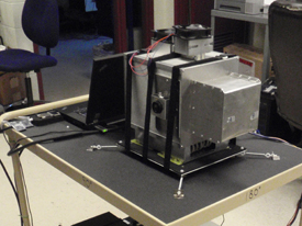
The new Polaris gamma ray detector can pinpoint the location of special nuclear materials, such as those used for dirty bombs or nuclear weapons. Image credit: Zhong He

ANN ARBOR, Mich.— A table-top gamma-ray detector created at the University of Michigan can not only identify the presence of dangerous nuclear materials, but can pinpoint and show their exact location and type, unlike conventional detectors.


“Other gamma ray detectors can tell you perhaps that nuclear materials are near a building, but with our detector, you can know the materials are in room A, or room B, for example,” said Zhong He, an associate professor in the Department of Nuclear Engineering and Radiological Sciences. 

“This is the first instrument for this purpose that can give you a real-time image of the radiation source. Not only can we tell you what material is there, but we can tell you where it is, and you can find it and walk towards it.”  (more…)

Read More