
Atomic force microscopy helps scientists to reveal the bond order and length of bonds within molecules
Technique can be used to study future devices made from graphene
Zurich, Switzerland – 14 Sep 2012: IBM scientists have been able to differentiate the chemical bonds in individual molecules for the first time using a technique known as noncontact atomic force microscopy (AFM).
The results push the exploration of using molecules and atoms at the smallest scale and could be important for studying graphene devices, which are currently being explored by both industry and academia for applications including high-bandwidth wireless communication and electronic displays.
“We found two different contrast mechanisms to distinguish bonds. The first one is based on small differences in the force measured above the bonds. We expected this kind of contrast but it was a challenge to resolve,” said IBM scientist Leo Gross. “The second contrast mechanism really came as a surprise: Bonds appeared with different lengths in AFM measurements. With the help of ab initio calculations we found that the tilting of the carbon monoxide molecule at the tip apex is the cause of this contrast.”
As reported in the cover story of the September 14th issue of Science magazine, IBM Research scientists imaged the bond order and length of individual carbon-carbon bonds in C60, also known as a buckyball for its football shape and two planar polycyclic aromatic hydrocarbons (PAHs), which resemble small flakes of graphene. The PAHs were synthesized by Centro de Investigacion en Quimica Bioloxica e Materiais Moleculares (CIQUS) at the Universidade de Santiago de Compostela and Centre National de la Recherche Scientifique (CNRS) in Toulouse.
The individual bonds between carbon atoms in such molecules differ subtly in their length and strength. All the important chemical, electronic, and optical properties of such molecules are related to the differences of bonds in the polyaromatic systems. Now, for the first time, these differences were detected for both individual molecules and bonds. This can increase basic understanding at the level of individual molecules, important for research on novel electronic devices, organic solar cells, and organic light-emitting diodes (OLEDs). In particular, the relaxation of bonds around defects in graphene as well as the changing of bonds in chemical reactions and in excited states could potentially be studied.
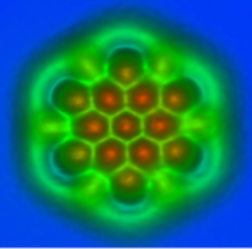
A nanographene molecule exhibiting carbon-carbon bonds of different length and bond order imaged by noncontact atomic force microscopy using a carbon monoxide functionalized tip. This molecule was synthesized at the Centre National de la Recherche Scientifique (CNRS) in Toulouse. Image credit: IBM Research - Zurich
As in their earlier research (Science 2009, 325, 1110) the IBM scientists used an atomic force microscope (AFM) with a tip that is terminated with a single carbon monoxide (CO) molecule. This tip oscillates with a tiny amplitude above the sample to measure the forces between the tip and the sample, such as a molecule, to create an image. The CO termination of the tip acts as a powerful magnifying glass to reveal the atomic structure of the molecule, including its bonds. This made it possible to distinguish individual bonds that differ only by 3 picometers or 3 × 10-12 meters, which is about one-hundredth of an atom’s diameter.
In previous research the team succeeded in imaging the chemical structure of a molecule, but not the subtle differences of the bonds. Discriminating bond order is close to the current resolution limit of the technique and often other effects obscure the contrast related to bond order. Therefore the scientists had to select and synthesize molecules in which perturbing background effects could be ruled out.
To corroborate the experimental findings and gain further insight into the exact nature of the contrast mechanisms, the team performed first-principles density functional theory calculations. Thereby they calculated the tilting of the CO molecule at the tip apex that occurs during imaging. They found how this tilting yields a magnification and the very sharp images of the bonds.
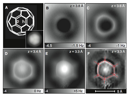
Measurements on C60. (A) C60 model. The bonds fusing a pentagon and a hexagon (p) are of smaller bond order compared with the bonds fusing two hexagons (h). (Inset) STM image (sample bias V = 0.2 V, current I = 2 pA, size 24 by 24 Å2). The molecule and tip are identical to those in (B) to (F). (B to E) AFM measurements showing frequency shift at different tip heights z (27) above C60/Cu(111) using a CO-functionalized tip. Image size 10 by 10 Å2, oscillation amplitude A = 0.36 Å, V = 0 V. (F) Laplace- filtered and flattened image of (E), used to measure the apparent bond length L′ (22). Image credit: IBM Research - Zurich
This research was funded within the framework of several European projects including ARTIST, HERODOT, CEMAS, the Spanish Ministry of Economy and Competitiveness and the Regional Government of Galicia.
The scientific paper entitled “Bond-Order Discrimination by Atomic Force Microscopy” by L. Gross, F. Mohn, N. Moll, B. Schuler, A. Criado, E. Guitian, D. Pena, A. Gourdon and G. Meyer, appears in Science, doi/10.1126/science.1225621 (14 September 2012).
IBM and nanotechnology
Scientists have been striving to “see” and manipulate atoms and molecules to extend human knowledge and push the frontiers of manufacturing capabilities to the nanometer regime. IBM has been a pioneer in nanoscience and nanotechnology ever since the development of the scanning tunneling microscope in 1981 by IBM Fellows Gerd Binnig and Heinrich Rohrer at IBM Research – Zurich.
For this invention, which made it possible to image individual atoms and later on to manipulate them, Binnig and Rohrer were awarded the Nobel Prize in Physics in 1986. The AFM, an offspring of the STM, was invented by Binnig in 1986. The STM is widely regarded as the instrument that opened the door to the nanoworld.
A new facility for world-class collaborative nanoscale research, the Binnig and Rohrer Nanotechnology Center was opened last year on the campus of IBM Research – Zurich. The Center is part of a strategic partnership in nanotechnology with ETH Zurich, one of Europe’s premier technical universities.

From left, Diego Peña, Alejandro Criado and Enrique Guitián with a model of the molecule we have prepared (DBNP) in our hands in the CIQUS lab. Image credit: Centro de Investigación en Química Biolóxica e Materiais Moleculares (CIQUS), Campus Vida, Universidade de Santiago de Compostela
View this timeline highlighting 30 years of nanotechnology at IBM Research.
*Source: IBM