
Berkeley Lab team shows metal-alloy catalysts give more control in nanowire fabrication.
A novel approach to growing nanowires promises a new means of control over their light-emitting and electronic properties. In a recent issue of Nano Letters, scientists from the U.S. Department of Energy’s Lawrence Berkeley National Lab (Berkeley Lab) demonstrated a new growth technique that uses specially engineered catalysts. These catalysts, which are precursors to growing the nanowires, have given scientists more options than ever in turning the color of light-emitting nanowires.
The new approach could potentially be applied to a variety of materials and be used for making next-generation devices such as solar cells, light emitting diodes, high power electronics and more, says Shaul Aloni, staff scientist at Berkeley Lab’s Molecular Foundry, a DOE user facility, and lead author on the study.
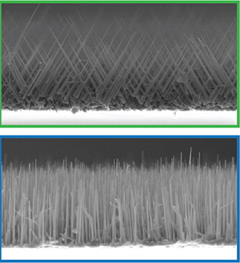
Nanowires grown using catalyst rich in gold (top) and nickel (bottom). Image credit: Berkeley Lab
Since the early 2000s, scientists have made steady progress in cultivating nanowires. Initially, early nanowire samples resembled “tangled noodles or wildfire-ravaged forests,” according to the researchers. More recently, scientists have found various conditions lead to the growth of more orderly nanowire arrays.
For instance, certain substrates on which the nanowires grow create conditions so that the nanowire growth orientation is dictated by the substrate’s underlying crystal structure. Unfortunately, this and other approaches haven’t been foolproof and some nanowires still go rogue.
Moreover, there is no simple way to grow different types of nanowires in the same environment and on the same substrate. This would be useful if you wanted to selectively grow nanowires with different electronic or optical properties in the same batch, for example.
“At the Molecular Foundry we are aiming to develop new strategies and add new tools to the bag of tricks used for nanomaterials synthesis,” says Aloni. “For years we were searching for cleverer ways to grow nanostructures with different optical properties in identical growth conditions. Engineering the catalyst brings us closer to achieving this goal.”
The researchers focused on nanowires made of gallium nitride. In its bulk (non-nanoscale) form, gallium nitride emits light in the blue or ultraviolet range. If indium atoms are added to it, the range can be extended to include red, essentially making it a broad-spectrum tunable light source in the visible range.
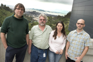
Research team from left to right: Shaul Aloni, Frank Ogletree, Virginia Altoe, Tevye Kuykendall. Image credit: Kelly Owen
The problem is that adding indium atoms puts the crystal structure of gallium nitride under stress, which leads to poorly performing devices. Gallium nitride nanowires, however, don’t experience the same sort of crystal strain, so scientists hope to use them as tunable, broad-spectrum light sources.
To achieve their control, the team focused on the catalysis which guide the nanowire growth. Normally, researchers use catalysts made of a single metal. The Berkeley team decided to use metallic mixtures of gold and nickel, called alloys, as catalysts instead.
In the study, the researchers found that the gallium-nitride nanowire growth orientation strongly depended on the relative concentration of nickel and gold within the catalyst. By altering the concentrations in the alloy, the researchers could precisely manipulate, even on the same substrate in the same batch, the orientation of the nanowires.
“No one had used bi-metalic catalysts to control growth direction before,” says Tevye Kuykendall, scientist at Berkeley Lab’s Molecular Foundry. Kuykendall says the mechanism driving the new growth process is not fully understood, but it involves the different tendencies of gold and nickel to align with various crystallographic surfaces at point where nanowires start to grow.
The researchers also showed that depending on the growth direction chosen, different optical properties were observed thanks to the crystal surfaces exposed at the surface of the nanowire. “One of the things that make nanostructures interesting, is that the surface plays a larger role in defining the material’s properties,” says Aloni. This leads to changes in optical properties not seen in larger-bulk materials, making them more useful.
Aloni says the team will next focus more on the chemistry of the different nanowire surfaces to further tailor the nanowire’s optical properties.
All aspects of the work were conducted at the Molecular Foundry, under the leadership of Aloni. Virginia Altoe imaged the nanowires using transmission electron microscopy in the imaging facility of the Molecular Foundry. Frank Ogletree, Molecular Foundry staff scientist, assisted in mapping the optical properties of the nanowires. And Kuykendall fabricated the wires in the Foundry’s inorganic facility. The methods and materials described in the paper are available free of charge to researchers from around the world through the Molecular Foundry’s user program.
This research was supported by the DOE Office of Science.
– By Kate Greene
*Source: Berkeley Lab