
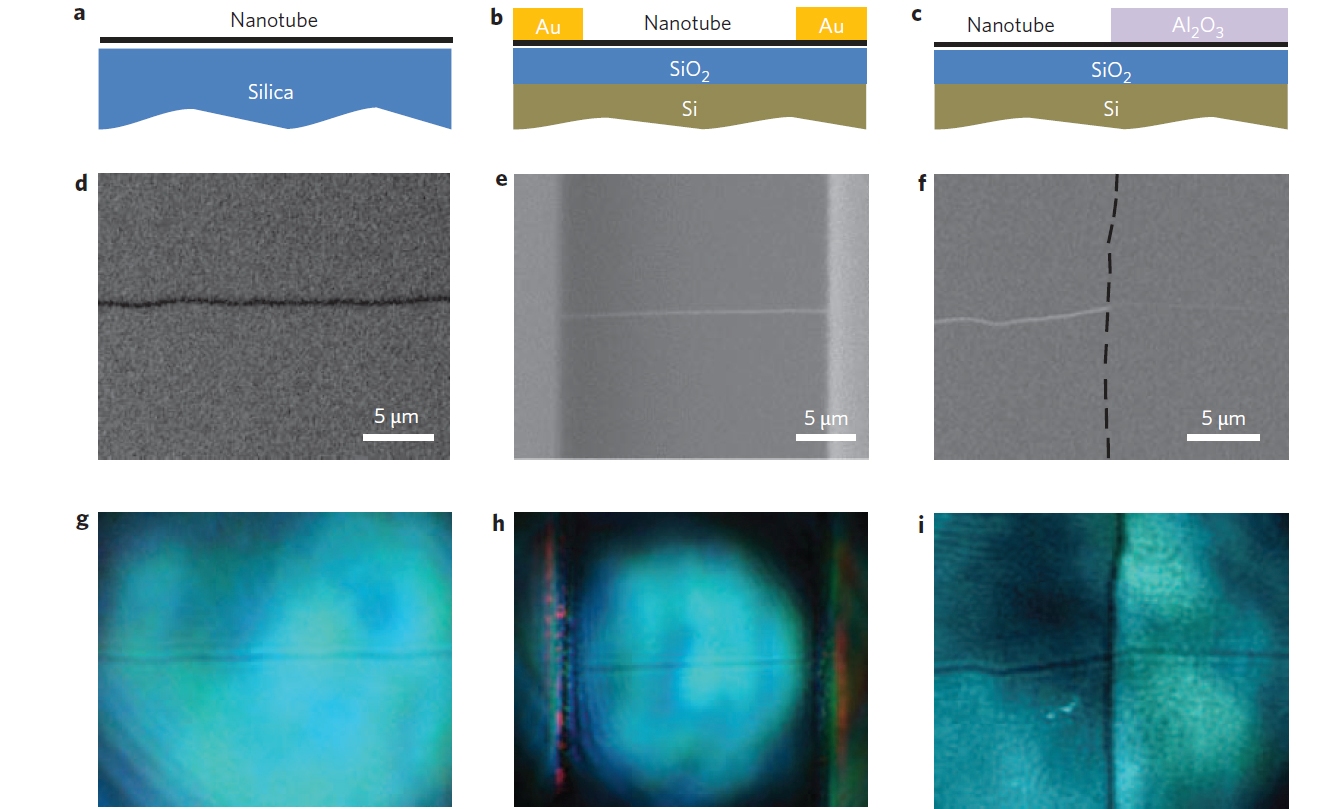
In this display showing optical imaging and spectroscopy of an individual nanotube on substrates and in devices, (a–c) are schematics of a nanotube on a fused-silica substrate, in a field-effect transistor device with two gold electrodes, and under an alumina dielectric layer; (d–f) are SEM images and (g-i) are direct optical images of these individual nanotubes. Image credit: Berkeley Lab (Click image to enlarge)
(Visited 188 times, 1 visits today)